
Forward Converter Calculator
This professional tool designs Forward Converters, a robust isolated topology derived from the Buck converter. It supports Single-Switch (with Reset Winding or RCD) and Two-Transistor configurations.
Use this calculator to determine transformer turns ratio, output inductance, and critical component voltage stress for your power supply design.
Configuration
Input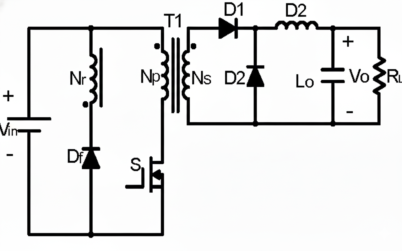
Design Analysis
CCMComponent Stress
Forward Topology Comparison
Choosing between Single-Switch and Two-Transistor Forward designs.
| Feature | Single-Switch (Reset) | Two-Transistor |
|---|---|---|
| Switch Voltage Stress | 2 × Vin (High) | 1 × Vin (Low) |
| Complexity | Low (1 FET) | Medium (2 FETs + High Side Drive) |
| Power Range | Up to 150W | 150W – 500W+ |
| Leakage Energy | Dissipated or Reset | Recycled to Input (Efficient) |
Key Design Formulas
Turns Ratio (n)
n = (Vin_min × Dmax) / (Vout + Vf)
Determines the step-down ratio. Typically Dmax is set to 0.45.Output Inductance (Lout)
Lout = (Vout × (1 – D)) / (fsw × ΔIL)
Sized to limit current ripple (ΔIL) to 20-40% of Iout.Switch Voltage (VDS)
Single Switch: ~2 × Vin
Two-Transistor: ~1 × Vin
How to Use
Choose Topology
Select Single-Switch for lower power/cost, or Two-Transistor for higher power and lower voltage stress on the switches.
Set Input/Output
Define your input voltage range and output requirements. The calculator automatically estimates the turns ratio (n) based on your target duty cycle.
Check Stress
Review the Switch VDS. In Single-Switch designs, this can be 2x or 3x the input voltage. Ensure your MOSFET is rated for it.