
Buck Converter Designer
Professional design tool for Step-Down (Buck) Converters. Calculates Inductor Sizing, critical Input Capacitor RMS Current, and Component Stress for reliable high-efficiency power supplies.
Specs & Margins
Input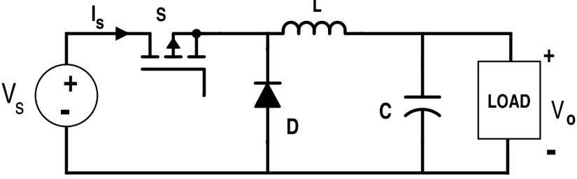
Design Analysis
CCM ModeBuck Converter vs LDO
Why choose a Switching Regulator (Buck) over a Linear Regulator (LDO)?
| Feature | Buck Converter | LDO (Linear) |
|---|---|---|
| Efficiency | High (80-95%) | Low (Vout/Vin) |
| Heat Generation | Low (Cold) | High (Hot) |
| Complexity | Medium (L, C, Diode) | Simple (Cap only) |
| Use Case | High Power / Big Step-Down | Low Noise / Small Step-Down |
Physics Explained
Input Capacitor Stress
In a Buck converter, the input current is pulsed. The input capacitor must handle significant RMS Ripple Current, roughly 50% of Iout at 50% duty cycle.
Component Stress
Unlike Boost converters, the MOSFET and Diode in a Buck converter must withstand Vin (plus ringing spikes), not just Vout.
LC Resonance
Buck converters have a double pole at fLC. The control loop bandwidth is usually set between fLC and fsw/10.
How to Use
Set Operating Point
Define Input (High) and Output (Low) voltages. Ensure Vin > Vout.
Check Input Cap
Pay close attention to the Input Cap IRMS result. Use low-ESR ceramic capacitors (X7R/X5R) to handle this heating.
Verify Stability
Note the fLC (Resonant Frequency). Your compensation network needs to handle the phase drop occurring at this frequency.